by Robert Richardson, Senior Engineer, dB Control
Pulsed RF amplifiers are an integral part of many modern applications – including radar, electronic warfare (EW), medical imaging systems, and military communication. The accuracy of these systems relies on the fidelity of the pulsed RF signal. Specifically, a pulsed RF amplifier should behave as closely to an ideal amplifier as possible (in which the output of the amplifier perfectly represents the input signal). Any signal found at the output of an amplifier that is not present at the input is considered a spurious signal. The result? These signals may show up as false targets or blurred images in radar and medical systems, or bit errors in communication systems, which compromise reliability. Likewise, spurious signals can appear in adjacent frequency channels and cause additional challenges.
Some systems can tolerate spurs, depending on their amplitude and distance from the carrier. Design engineers can certainly determine the maximum level and frequency of spurs a particular system can accept. But in industries where reliability is essential and performance/accuracy requirements increase, designers must figure out how to reduce spurious levels in the first place.
Traveling wave tubes (TWTs) are a great choice for pulsed RF systems that require high output power, wide/instantaneous bandwidth, and good power efficiency. Like all real-world amplifiers, TWT Amplifiers (comprised of a TWT and a high-voltage power supply) introduce some non-ideal traits on the amplified signal, which results in spurious components. Reducing these spurs will typically improve system accuracy and reduce potential negative effects. Design engineers whose systems have strict spurious requirements can examine the source of spurs in TWTAs and reduce them using one of two techniques – “nesting” and “pulse shaping.”
What Causes Spurs in TWTAs?
Spurious components in TWTAs are often a result of amplitude and phase modulation of the RF signal. These types of modulation occur when the velocity of the TWT electron beam is varied during the RF amplification. Variations in the TWT cathode and grid voltages have the greatest effect on the velocity of the electron beam. Cathode voltage variations typically create phase modulation and some amplitude modulation. Grid or FE voltage variations mainly create amplitude modulation with some phase modulation. It’s important to note that some TWTAs generate white noise which can also contribute to spurious components. This noise is created by the TWT, and the high voltage power supply (HVPS) cannot compensate or eliminate it.
Another cause of TWTA spurious components comes from the HVPS inverter and line voltage frequencies. TWTA power supplies use an inverter to convert the line voltage to the high voltage required by the TWT. The inverter causes spurious components at the inverter’s switching frequency. In addition, power supplies that use AC line voltage will have spurious components at the line voltage frequency (typically 60 or 400 Hz). TWT power supplies can be designed to reduce these spurious components through strict voltage regulation – or in some applications – by shutting off the inverter during the RF pulse (blanking).
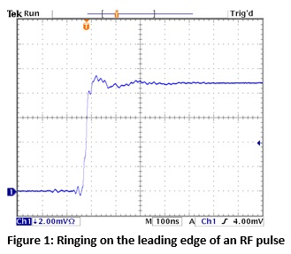
Both CW and pulsed amplifiers will create spurious modulations. TWT power supplies are designed to minimize variations in the cathode and grid voltages to reduce spurious components, but even the most well-designed pulsed system will have some amount of “ringing” present at the beginning and ending of the RF pulse. (Figure 1) Although there is no way to completely eliminate the ringing in a pulsed RF amplifier, nesting or pulse shaping can reduce the spurious signals they create.
How to View Spurious Signals
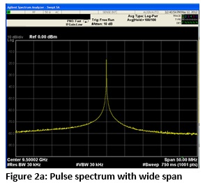
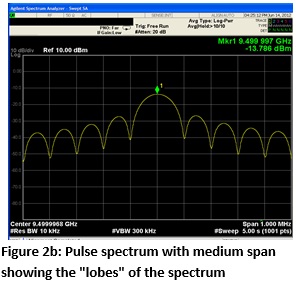
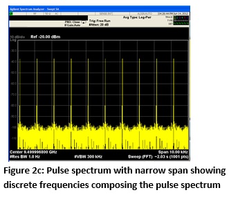
Spurious signals in an RF pulse are observed by viewing the frequency spectrum of the pulse on a spectrum analyzer. A pulsed RF signal is a composite of an infinite number of discrete frequencies at predictable amplitudes and distribution. When an ideal RF pulse is observed in the frequency domain, the line spectrum amplitude follows a sin(X)/X envelope (Figure 2). When viewed with a wide span, the spectrum looks like a CW signal with skirts on both sides of the carrier. Decreasing the span and zooming in on the carrier shows the “lobes” of the spectrum, and a further decrease in span resolves the spectrum into discrete frequencies centered around the carrier and separated by a distance equal to the frequency of the pulse train. The spurs examined in this document will all be viewed with a wide span.
Spurs in the RF pulse are seen as deviations from this envelope. In RF amplifiers, the value of these spurious signals are measured with respect to the intended amplified signal. For example, if the RF carrier is a single frequency with a magnitude of 70 dBm, and a spurious signal is found measuring 40 dBm, that spur would be measured as -30 dBc (dB below the carrier). The lower the spur is from the carrier, the greater the performance.
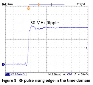
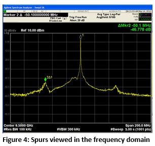
Spurious signals greater than 1 MHz can often be viewed in the time domain as amplitude ripple on the pulse. Figure 3 shows the rise of a 50 uS X-band pulse in the time domain with a ripple frequency around 50 MHz on the leading edge of the pulse. Figure 4 shows this 50 uS, 1.0 kHz pulse train viewed in the frequency domain with -46 dBc spurs visible at 50.1 MHz.
Reducing Spurs Through RF Nesting
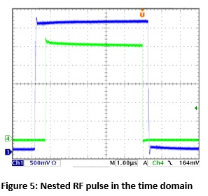
“Nesting” is a practice that places a short delay between enabling the TWT and the start of the RF pulse. This provides a settling time for the TWTA to stabilize the electron beam in the tube before amplifying the RF. Typical delay times are in the hundreds of nanoseconds. Figure 5 shows this technique in the time domain. The blue trace represents the TWT beam being enabled and the green trace is the nested RF pulse.
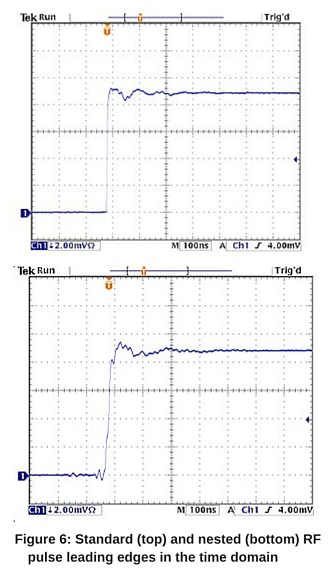
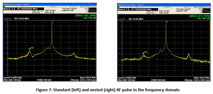
This technique was applied to the 50 MHz spurious components seen in Figure 1 with a 500nS delay for the RF pulse. The benefits are shown in Figures 6 and 7. The standard RF pulse in Figure 6 shows a noticeable 50 MHz (20 nS period) ringing during the first 500 nS of the pulse. In the frequency domain this ringing results in a spurious component separated from the carrier by 50 MHz (as seen in Figure 7). With the RF pulse nested, the ripple viewed in the time domain is significantly reduced. In the frequency domain, the 50 MHz spur has been reduced by 9 dB and the overall spectrum is a better representation of the original pulse.
The amount of delay used in this technique determines its ability to reduce spurious components. Most of the benefit will be realized with under a microsecond of delay. Typical pulsed TWTs have a maximum duty cycle at which they may operate and the trade off with nesting is that it cuts into the duty cycle budget.
Reducing Spurs Through RF Pulse Shaping
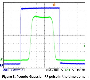
Another technique for reducing spurs is to shape the RF pulse into a pseudo-Gaussian shape by slowing the rise and fall time of the RF signal at the input of the amplifier. This allows time for the cathode, grid and electron beam to stabilize. This also reduces the ringing involved with the step response of the RF pulse. Additionally, the pulse is no longer a pure square wave, so the frequency spectrum contains fewer components. Typical rise and fall times for this technique are in the low microseconds. Figure 8 shows this technique in the time domain. The blue trace represents the TWT beam being enabled and the green trace is the pseudo-Gaussian shaped RF pulse.
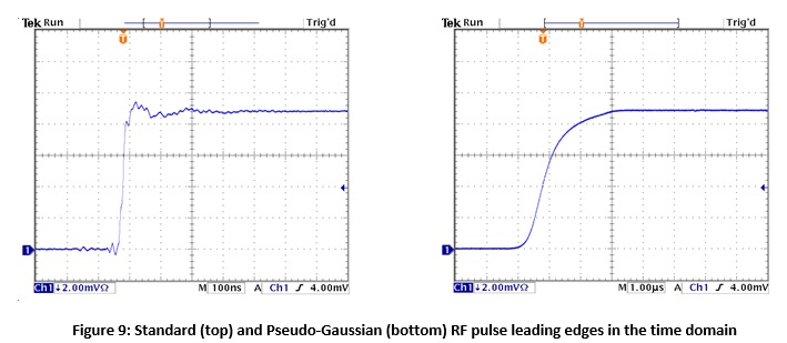
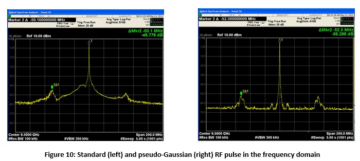
This technique was applied to the example shown in Figure 8 using a 1.5 uS rise and fall time. The benefits are shown in Figures 9 and 10. In the time domain, the 50 MHz ringing on the front end has been significantly reduced. In the frequency domain, the 50 MHz spurs have been reduced by 9.5 dB. Also note that the spectrum of the pulse in the frequency domain has narrowed. This provides a clearer picture of the carrier and the spurs.
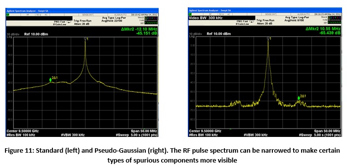
It’s also important to note what is happening closer to the carrier in the frequency domain. Figure 11 shows the unaltered RF pulse with spurs located 12.2 MHZ from the carrier at -45.15 dBc. This spur is located on the slopes of the spectrum. At this offset from the carrier, the amplitude of the frequencies that make up the pulse are large and the spurious component is summed with the pulse components. This can create the false impression that the spur is larger than it really is. Examining the area in greater detail reveals that the spur and the pulse component are in fact two discrete frequencies. Unfortunately, the limitations of test equipment make this distinction difficult to observe. With a pseudo-Gaussian RF pulse, the spectrum is narrowed and the spurs can be clearly seen. Figure 11 illustrates an 18.3 dB decrease compared to the previously measured spur level.
The rise and fall time used for this technique determines the effectiveness in reducing spurious components and enhancing visibility in the frequency domain. Most of the benefit will be realized with a rise time of under a microsecond. The trade off with RF pulse shaping is that it also cuts into the duty cycle budget of the TWT.
Balancing Spurious Output and Duty Cycle Budget
RF nesting and pulse shaping offer design engineers two effective techniques to improve spurious levels in pulsed RF amplifiers. Determining which method will produce the best results depends on the system. Using one of these two techniques enables pulsed RF systems with strict spurious requirements to benefit from the high power advantages of TWTAs. While it’s true that the design engineers will need to engage in a delicate, but doable, balance between spurious output and duty cycle budget by examining system requirements and determining how to reduce spurious components, doing so will ensure delivery of high output power, wide/instantaneous bandwidth and power efficiency that only TWTAs can provide.
Robert Richardson is a senior engineer at dB Control (Fremont, CA). For more information about dB Control’s capabilities, please visit www.dbcontrol.com, call (510) 656-2325 or email info@dbcontrol.com.
This article originally appeared in the April 2016 issue of Microwave Product Digest.